
signal integrity in complex printed circuit board assembly designs
Ensuring signal integrity in complex printed circuit board assembly (PCBA) designs is critical for maintaining the performance, reliability, and functionality of electronic devices. Signal integrity refers to the ability of signals to propagate accurately and efficiently through the PCB without degradation or interference. Achieving and maintaining signal integrity requires careful consideration of various factors throughout the design, manufacturing, and testing phases.
One fundamental aspect of ensuring signal integrity in printed circuit board assembly designs is proper impedance matching. Impedance mismatches between signal traces, vias, and components can lead to signal reflections, ringing, and other forms of distortion. To mitigate impedance mismatches, designers must carefully calculate and control the characteristic impedance of transmission lines, taking into account factors such as trace geometry, dielectric properties, and layer stackup configuration. Utilizing controlled impedance routing techniques and adhering to design guidelines provided by PCB layout software can help ensure consistent signal transmission and minimize signal degradation.
Furthermore, minimizing electromagnetic interference (EMI) and electromagnetic compatibility (EMC) issues is essential for preserving signal integrity in complex PCBA designs. EMI can arise from various sources, including high-speed digital signals, switching power supplies, and radio frequency (RF) components. Designers must employ techniques such as proper grounding, shielding, and signal routing to reduce the risk of EMI and ensure that sensitive signals remain unaffected by external interference. Shielding sensitive components, separating analog and digital signal traces, and implementing low-noise power distribution networks can help mitigate EMI and maintain signal integrity.
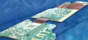
How do you ensure signal integrity in complex printed circuit board assembly designs?
Additionally, managing signal integrity in high-speed PCB designs requires careful attention to signal integrity analysis and simulation. Tools such as signal integrity analysis software and electromagnetic field simulators enable designers to predict and assess the behavior of signals in complex PCB layouts. By performing pre-layout and post-layout simulations, designers can identify potential signal integrity issues, such as crosstalk, skew, and jitter, and implement appropriate design modifications to address them. Iterative simulation and validation are essential for optimizing signal integrity and ensuring that design requirements are met.
Moreover, proper power distribution and decoupling are critical for maintaining signal integrity in complex PCBA designs. High-speed digital components and integrated circuits (ICs) require stable and noise-free power supplies to operate correctly. Designers must carefully plan power distribution networks, minimize voltage droops and spikes, and strategically place decoupling capacitors to provide clean power to sensitive components. Proper power integrity analysis and simulation are essential for verifying the effectiveness of the power distribution system and ensuring that voltage fluctuations do not compromise signal integrity.
Furthermore, thorough testing and validation are essential steps in ensuring signal integrity in complex PCBA designs. In addition to functional testing, designers should perform signal integrity testing using high-frequency oscilloscopes, time-domain reflectometers (TDRs), and network analyzers to verify signal quality and integrity. Signal integrity testing helps identify any potential issues that may have been overlooked during the design phase and allows for corrective actions to be taken before mass production.
In conclusion, ensuring signal integrity in complex printed circuit board assembly (PCBA) designs requires a comprehensive approach that encompasses careful planning, analysis, simulation, and testing. By considering factors such as impedance matching, EMI/EMC mitigation, signal routing, power distribution, and testing methodologies, designers can optimize signal transmission and minimize the risk of signal degradation or interference. Adhering to best practices and leveraging advanced design tools and techniques are essential for achieving high-performance and reliable PCBA designs in today’s increasingly interconnected and high-speed electronic systems.